My Journey Learning KiCad
Struggling to learn PCB design? Here is how Fedevel Academy’s beginner course helped me finally bridge the gap between messy breadboards and professional, manufactured hardware.
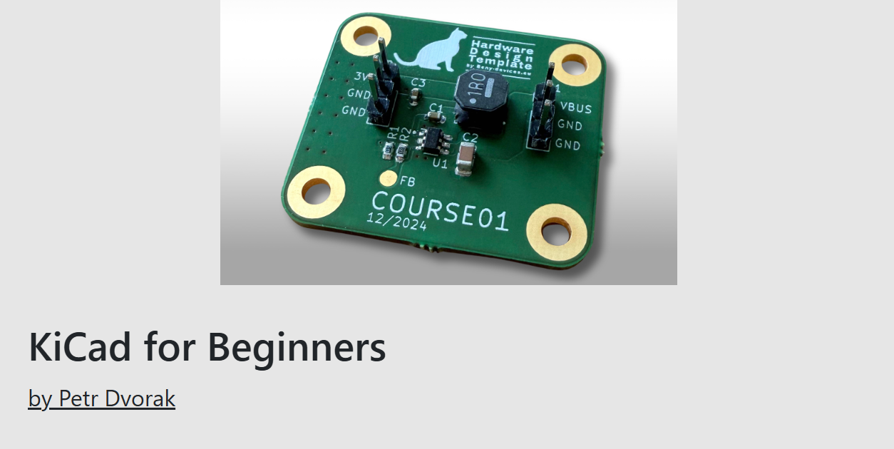
For a long time, transitioning from wiring up messy breadboards to designing a proper Printed Circuit Board (PCB) felt like a massive hurdle. Every time I opened CAD software, the sheer number of menus, the missing libraries, and the intimidating "blank canvas" stopped me in my tracks.
That just changed. I recently completed the KiCad for Beginners course by Fedevel Academy, taught by Petr Dvorak, and I wanted to share a quick, honest review of the experience.
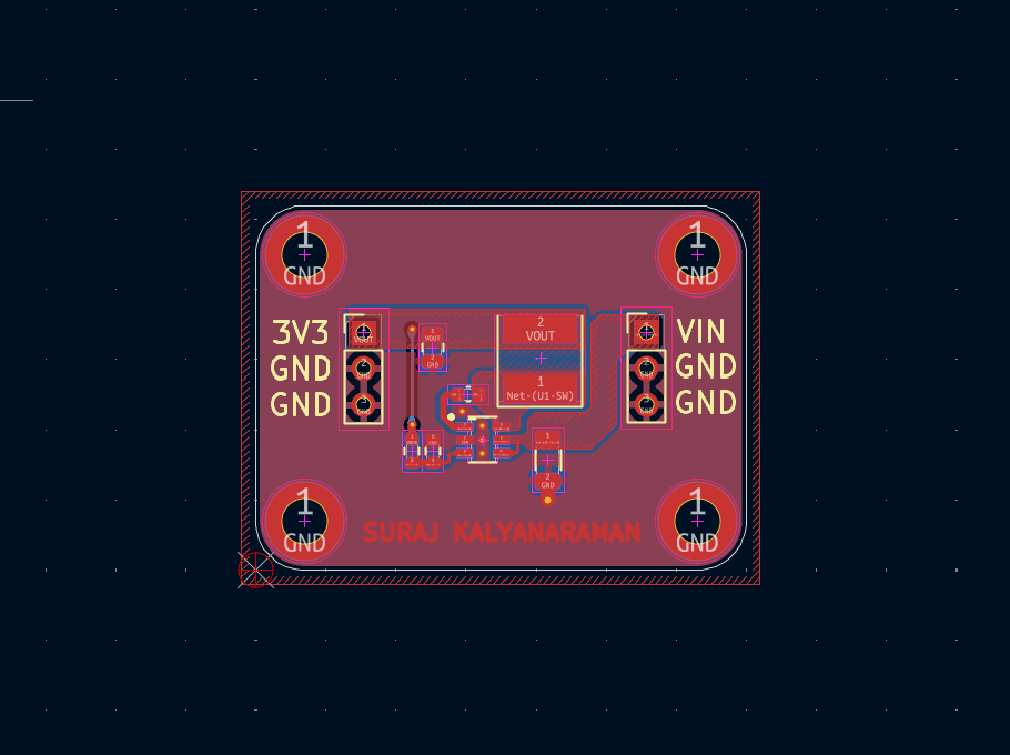
What I Loved About It: A Practical Workflow
The biggest strength of this course is that it skips the dry, theoretical lectures and gets you building immediately. You don't just learn what the buttons do you learn the actual industry workflow. Over the 7 lessons, we designed a complete, functional switching power supply from scratch.
Here is a breakdown of how the course transformed my approach to hardware design:
1. Building a Solid Foundation (Libraries & Footprints) If you’ve ever tried to learn PCB design, you know the frustration of placing a part only to realize it doesn't have a footprint. Instead of getting lost in default libraries, Petr taught us how to build our own. We started by creating custom schematic symbols and drawing precise footprints for our switching IC and passive components. We even linked 3D models to them. Learning to manage project specific libraries meant that when it was time to actually design the circuit, everything just worked.
2. Schematic Capture to PCB Layout Once our libraries were set up, we moved into schematic capture. We logically wired our signal paths, assigned power nets, and ran Electrical Rule Checks (ERC) to ensure the circuit was sound.
Pushing the design to the PCB editor was where the magic happened. Petr guided us through:
Defining the physical board outline, adding rounded corners, and placing mounting holes.
Strategically placing components to keep the high-frequency switching loops tight (crucial for a switching regulator!).
Routing tracks and pouring copper polygons to create solid ground and power planes, which handles the current and reduces electrical noise.
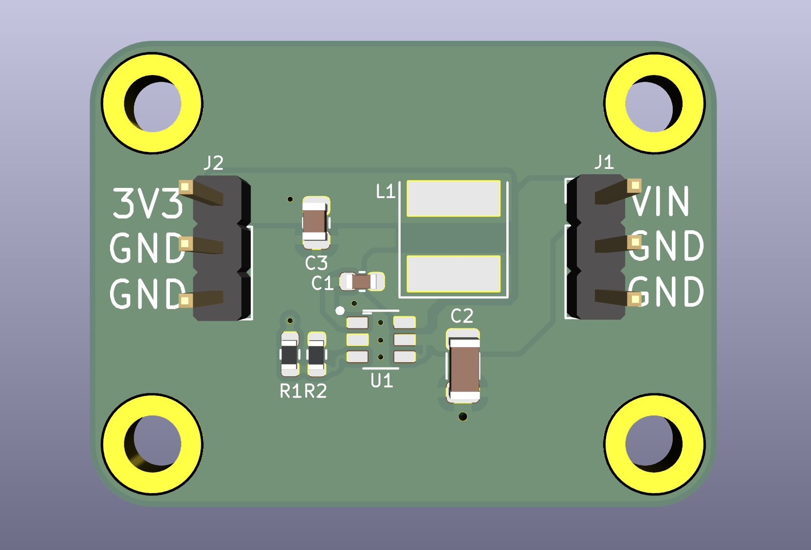
3. Manufacturing Handoff & Prototype Testing Designing a board on a screen is fun, but getting it manufactured is the ultimate goal. The course demystified the handover process to a fab house (like NextPCB). We generated the exact CAM data needed for real-world manufacturing: Gerber files, drill files, Bills of Materials (BOM), and Pick and Place files for automated assembly.
But the course didn't stop at the software. The final module covered the most nervewracking part of hardware engineering: the bring up. We went through the methodical process of testing the physical prototype safely first without a load to verify voltages, and then with a resistive load to simulate real-world usage.
My Honest Feedback
If you are someone who wants to get into PCB design but feels overwhelmed by where to start, I cannot recommend this course enough.
It is intensely practical and bridges the gap between software theory and manufacturing reality. It gave me the confidence to know that I can open KiCad today, start a brand new project, and successfully see it through to manufacturing. A huge shoutout to Petr and Fedevel Academy for putting together such an accessible and high-quality course.
I’m already looking forward to applying these skills to my next hardware project. Stay tuned!
What's Next?
Now that I have the foundational PCB workflow down, I’m already starting my next hardware project: A flexible PCB (FPC) smart shoe sole. I’ll be designing a flexible sensor carrier with 4 Force Sensitive Resistors (FSRs) to track gait analysis and foot pressure. It’s going to require learning strict flex-PCB design rules (no sharp corners, teardrops, hatched polygons), and I can’t wait to get it manufactured and test it in the real world.
Comments
Replies to this content are sent to the original instance.
Log in to comment.
No replies received yet.